From Sand to Silicon: How Computer Chips Are Made
The chip inside your laptop started as ordinary beach sand. That sentence sounds like a bad metaphor, but it's literally true — silicon, the second most abundant element in Earth's crust, is refined from silicon dioxide, the same compound that makes up quartz and common sand. What happens between that raw material and the processor running billions of calculations per second is one of the most complex manufacturing processes humans have ever devised.
What Is a Computer Chip, Really?
More Than Just a Piece of Metal
A computer chip — technically an integrated circuit — is a collection of transistors, capacitors, and resistors etched onto a thin slice of semiconductor material. Modern chips pack billions of these components into a space smaller than your thumbnail. The transistors act as microscopic switches, flipping between on and off states billions of times per second to process information in binary code.
The counterintuitive part: the 'chip' you see on a circuit board is mostly packaging. The actual silicon die inside is often smaller than a fingernail. That black plastic or ceramic housing is just there to protect the die and give it connectable pins or pads.
Silicon is the material of choice not because it conducts electricity well — metals do that better — but because its conductivity can be precisely controlled. Add certain impurities and it conducts. Remove them and it insulates. That tunability is everything in transistor design.
How Silicon Gets Purified — The Surprisingly Violent First Step
From Gritty Ore to 99.9999999% Pure Crystal
Raw silicon dioxide is first reduced in an electric arc furnace at temperatures above 1,400 degrees Celsius, producing metallurgical-grade silicon that's roughly 98–99% pure. That sounds impressive until you realize chipmakers need silicon that's 99.9999999% pure — nine nines, in industry shorthand. A single stray atom of the wrong element in the wrong place can ruin a transistor.
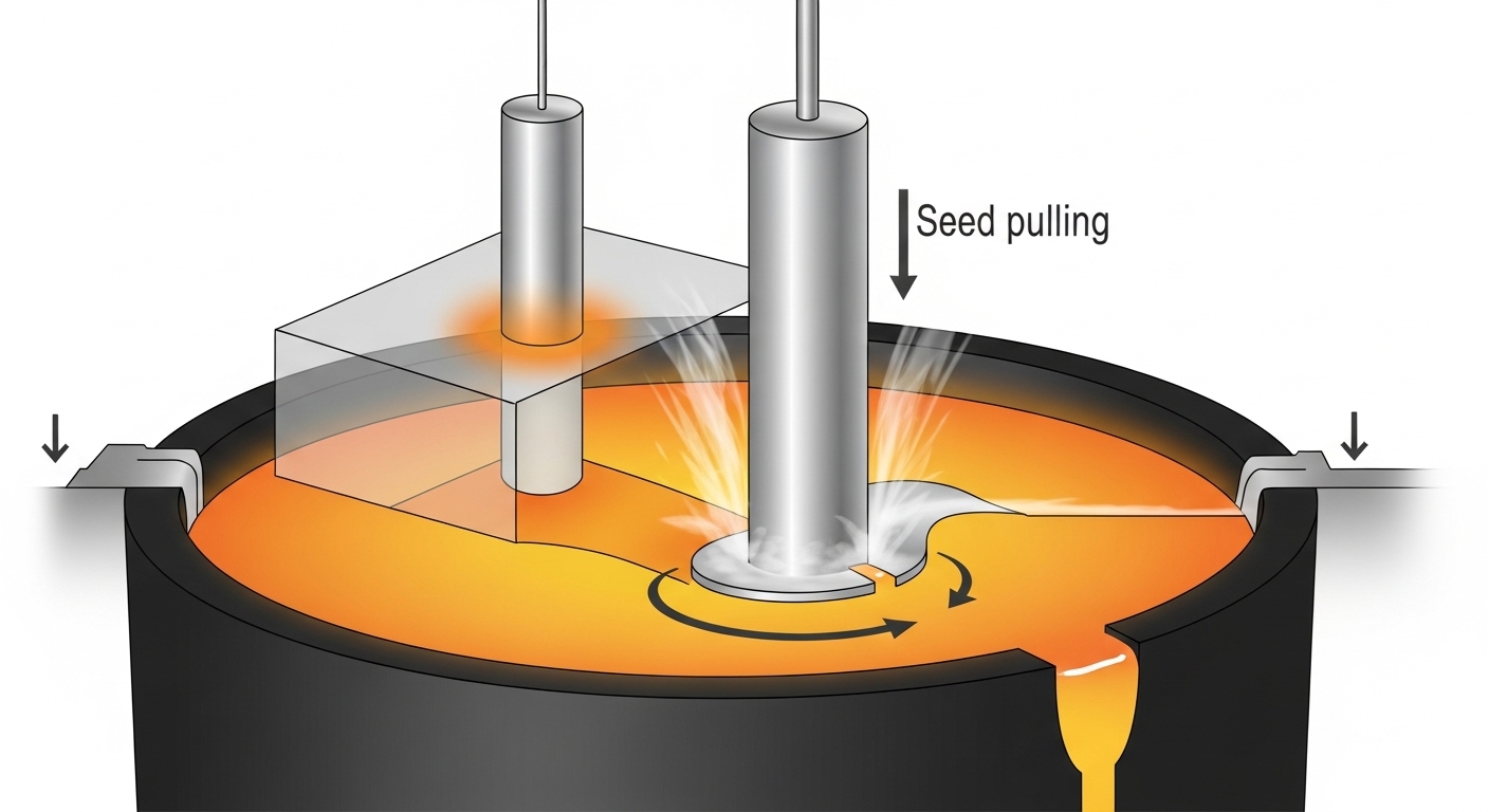
Getting there requires a process called the Siemens method, where silicon is converted to trichlorosilane gas, purified through distillation, then decomposed back into ultra-pure polysilicon rods. Those rods are then melted and slowly pulled into a single cylindrical crystal using the Czochralski process — a technique where a seed crystal is dipped into molten silicon and rotated upward at a carefully controlled rate. The result is a large, cylindrical ingot of near-perfect silicon crystal, sometimes over a meter long.
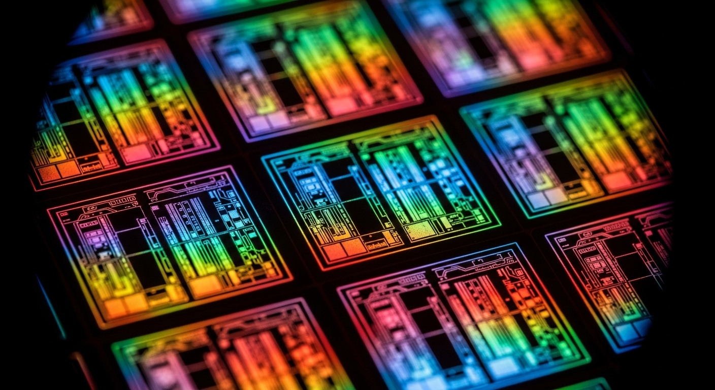
That ingot is then sliced into thin discs called wafers using diamond-edged wire saws. A standard wafer used in leading-edge fabrication today is 300mm in diameter — about the size of a dinner plate — and sliced to a thickness of less than a millimeter.
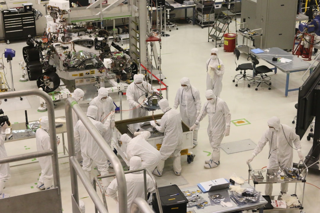
A single particle of dust landing on a wafer during fabrication can destroy dozens of chips. Chipmaking cleanrooms are tens of thousands of times cleaner than a hospital operating room.
How Chip Patterns Are Printed — The Physics of Extreme Light
Photolithography: Drawing With Light at Nanometer Scale
Once you have a polished wafer, you need to print the circuit design onto it. This is done through photolithography — essentially a high-precision photography process. The wafer is coated with a light-sensitive chemical called a photoresist, then exposed to light through a mask (a stencil of the circuit pattern). Where light hits the photoresist, the chemistry changes, allowing certain areas to be chemically etched away and others to remain.
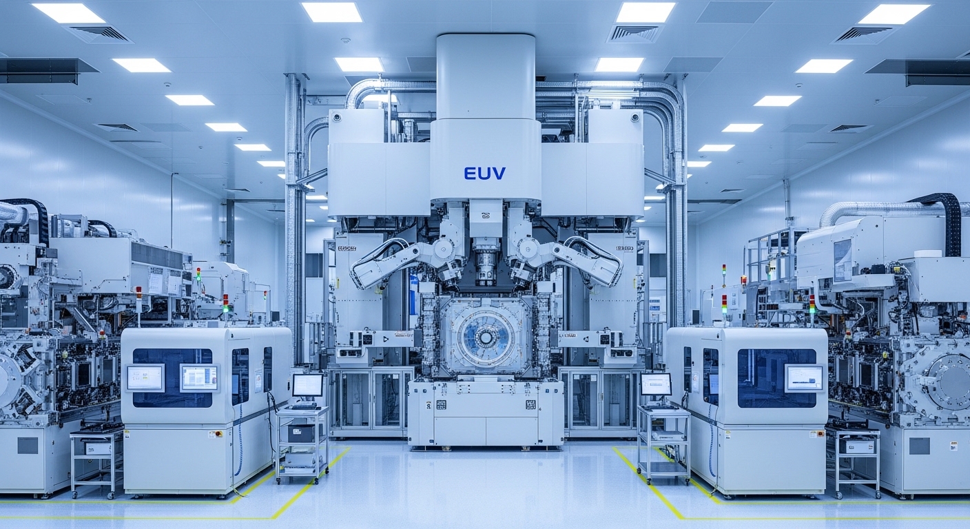
The challenge is scale. Modern transistors are measured in nanometers — a few nanometers is roughly the width of a handful of atoms side by side. Visible light has wavelengths far too long to print features that small. The industry's solution, developed over decades, is Extreme Ultraviolet (EUV) lithography, which uses light with a wavelength of just 13.5 nanometers. Generating that light requires firing a high-powered laser at tiny droplets of molten tin, creating a plasma that emits EUV radiation. The machines that do this — built primarily by the Dutch company ASML — weigh around 180 tonnes and cost upwards of 150 million dollars each.
This process is repeated dozens of times per wafer, each pass adding a new layer of the circuit — transistors, then wiring, then insulation, then more wiring. A finished chip may have over 100 distinct layers stacked on top of each other.
Doping: Deliberately Contaminating Silicon
Between lithography steps, specific regions of the silicon are 'doped' — implanted with carefully chosen impurity atoms like phosphorus or boron using ion beams. This is what creates the p-type and n-type semiconductor regions that make transistors work. The precision required is extraordinary: ion beams must deposit atoms at exact depths and concentrations, measured in parts per billion.
Testing, Dicing, and Packaging — The Final Gauntlet
Why Most Chips Don't Survive
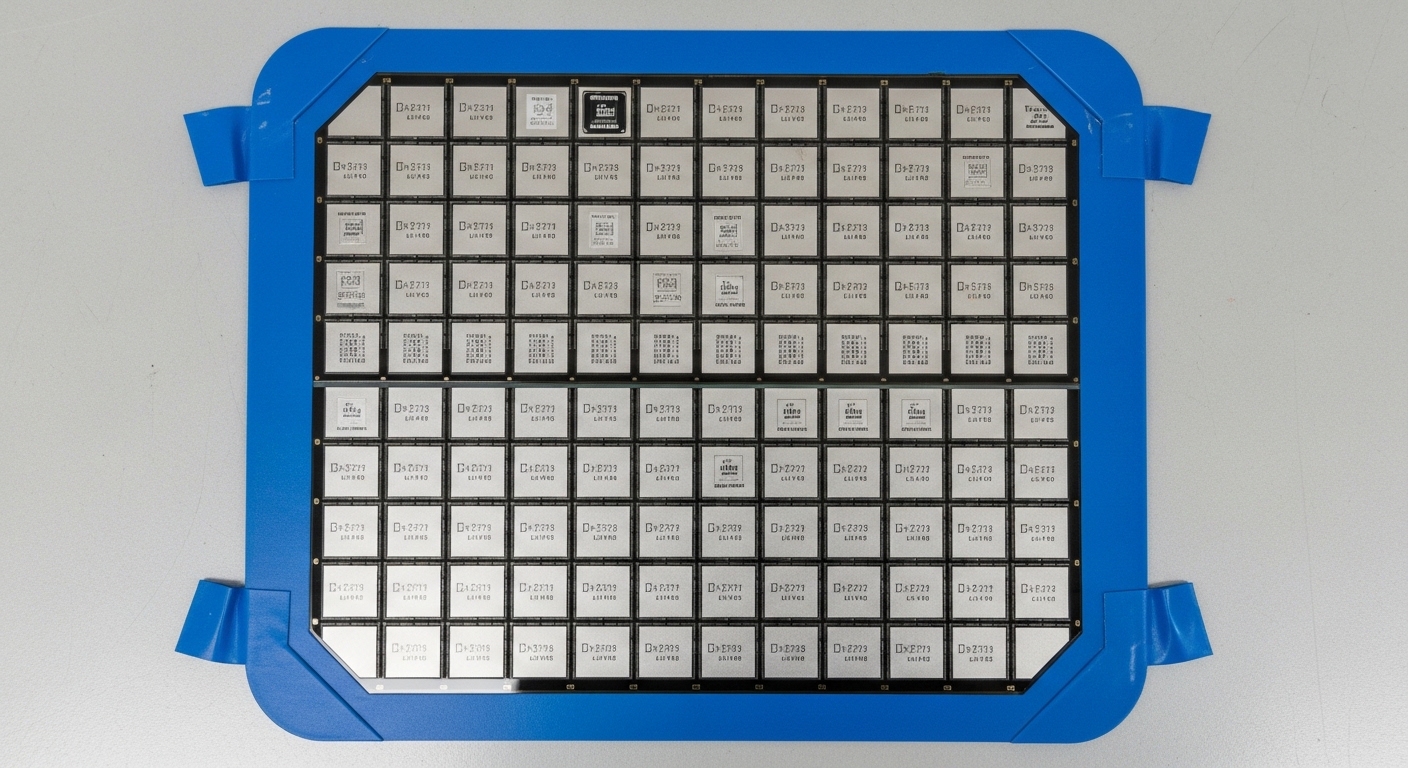
After fabrication, every chip on the wafer is tested electronically while still part of the wafer — a process called wafer probing. Tiny needles make contact with each die's test pads and run thousands of electrical checks. Chips that fail are marked with ink or logged digitally. Yields — the percentage of working chips per wafer — are a closely guarded metric in the industry. For leading-edge processes, early yields can be surprisingly low, sometimes below 50% when a new node first enters production.
Passing chips are then separated from the wafer by dicing — cutting along the grid lines with a diamond saw or laser. Individual dies are picked up, placed onto substrates, and wire-bonded or flip-chip bonded to connect the die's contact points to the package's external pins. The whole assembly is then encapsulated in epoxy or ceramic.
Final testing happens again after packaging, this time at temperature extremes — chips are tested hot and cold to catch failures that only appear under thermal stress. A chip that passes all tests gets binned by performance: the fastest examples become the flagship product, slower ones become budget variants. That's why the same physical chip design often appears at multiple price points.
Chip 'binning' means two processors with identical silicon can sell for vastly different prices — the only real difference is how fast they ran during the final test.
Why Chip Manufacturing Matters Beyond Your Laptop
The Geopolitics Hidden Inside Every Device
The global chip supply chain is one of the most concentrated in any industry. A handful of companies control critical steps: ASML holds a near-monopoly on EUV lithography machines. TSMC in Taiwan manufactures chips for most of the world's leading chip designers. A disruption at any single node — a natural disaster, a trade restriction, a factory fire — ripples across automotive, medical, consumer electronics, and defense industries simultaneously. The chip shortages that hit the auto industry in the early 2020s were a vivid demonstration of how fragile that chain can be.
Governments have taken notice. The United States, European Union, Japan, and South Korea have all launched significant subsidy programs to attract or retain semiconductor manufacturing capacity domestically. Building a leading-edge fab costs somewhere between 10 and 20 billion dollars and takes several years to construct and qualify — which means these policy bets won't pay off quickly.
(Opinion: There's something quietly unsettling about the fact that the devices billions of people depend on daily are produced by an industry concentrated in a handful of facilities, most of them within reach of geopolitical flashpoints. Diversifying that supply chain is genuinely one of the more important industrial policy challenges of this decade.)The physics of shrinking transistors is also approaching hard limits. At a few nanometers, quantum tunneling — where electrons pass through barriers they classically shouldn't be able to cross — becomes a real engineering problem, not a theoretical one. The industry's response has been to go vertical: stacking chips in 3D packages and redesigning transistor architectures rather than simply shrinking them further.

Frequently Asked Questions
How long does it take to make a computer chip from start to finish?
The full fabrication cycle for a leading-edge chip — from blank wafer to packaged, tested product — typically takes between two and four months. The lithography and deposition steps alone involve hundreds of individual process stages. This long cycle time is one reason chip shortages are so difficult to resolve quickly: you can't just flip a switch and get more chips next week.
Is the silicon in chips actually made from beach sand?
Technically yes, but with an important caveat. The silicon ultimately comes from silicon dioxide, the same compound found in quartz sand. However, chipmakers don't scoop up beach sand — they use high-purity quartz rock as the starting material, since beach sand contains too many contaminants. The chemistry is the same; the source material is more controlled.
Why can't chips just be made anywhere? What makes it so hard to build new fabs?
Building a fab requires not just the physical facility but an entire ecosystem: ultra-pure water supplies, vibration-isolated foundations, specialized gases, and a trained workforce that takes years to develop. The equipment itself has lead times of a year or more. Perhaps most critically, the process knowledge — the exact recipes for thousands of individual steps — takes years of trial and error to optimize. That accumulated expertise is genuinely hard to replicate quickly, regardless of how much money is available.
The gap between a grain of sand and a functioning processor is measured not just in distance or time, but in the accumulated knowledge of tens of thousands of engineers working across chemistry, physics, materials science, and precision optics. Every chip that ships is, in a quiet way, a small miracle of coordinated human expertise — one that most people hold in their hands without a second thought, until the supply chain breaks and suddenly nothing works.


Comments
Post a Comment